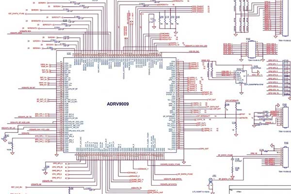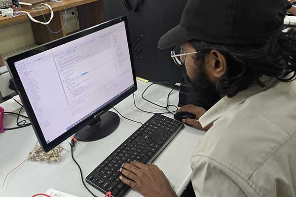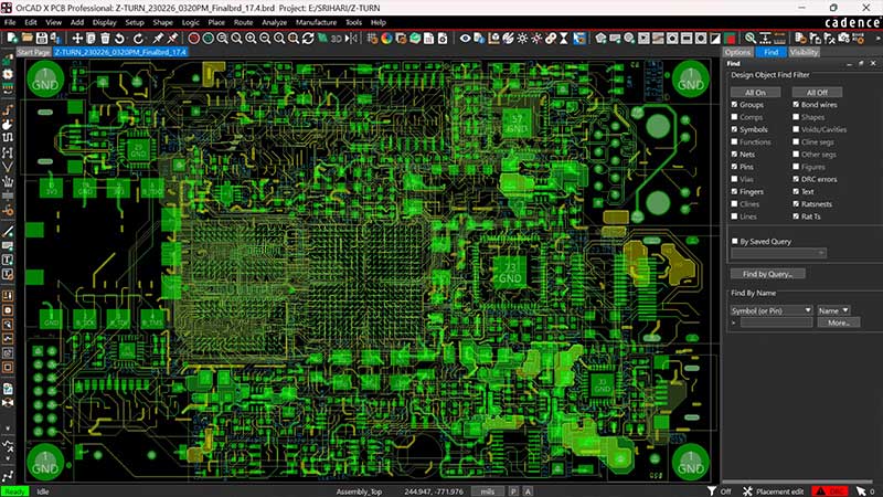
High-layer-count, high-speed boards fail in the layout stage as often as they do in schematic design. Our PCB design team runs full pre- and post-layout signal integrity and power integrity simulation on every controlled-impedance board we ship.
We design up to 22 layers in-house, with stack-up, impedance, and thermal analysis handled by the same engineers who will support the board through fabrication and bring-up.
Key capabilities
- Up to 20-layer, controlled-impedance stack-ups.
- Power integrity and plane analysis for high-current designs
- DFM review against IPC-2221/IPC-7520 before release
- Full pre-layout and post-layout signal integrity simulation
- Thermal analysis for power dissipation management
Our process
- Stack-up definition and impedance planning
- Placement and floor-planning for signal integrity
- High-speed routing with length-matching and via optimisation
- SI/PI simulation and design review
- DFM sign-off and fabrication release